PC Board milling (Isolation Routing)
KiCAD
In KiCAD
Starting with a fully-routed and verified PC board design.
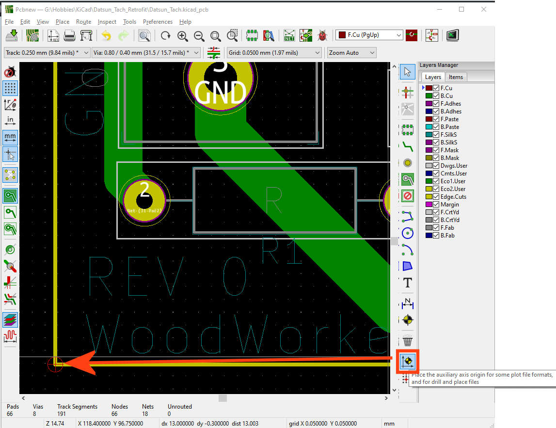
Place the origin (e.g. auxiliary axis) ![]() point (0, 0) for the drill and mill files.
point (0, 0) for the drill and mill files.
I typically put it at the ‘bottom left’ corner of my PC board outline.
This will be the 0, 0 point where milling will start – that is, this is the point where you will home your X and Y axis
Plot the “mill” and “drill” files.
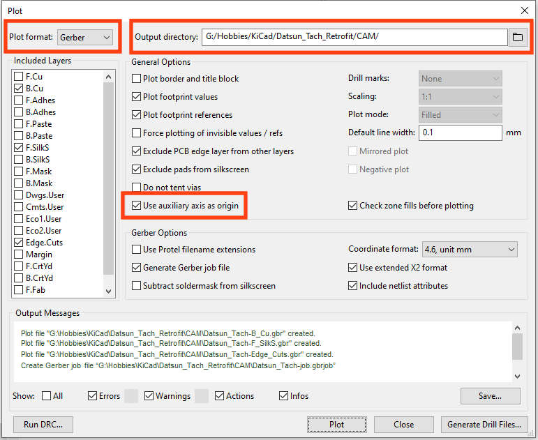
From Pcbnew, “Plot” the Gerber files ![]() .
.
Prepare the Plot page (Figure 4)
- Plot format: Gerber
- Make sure Output Directory is blank – KiCAD will store the Gerbers in the same directory as the Project files.
OR navigate to the file in which you want the files stored. I prefer to put the Gerber, drill and gcode files in a “CAM” subdirectory.. - Check Use auxiliary axis a origin
- Leave the Format as 4.6 (unit mm)
Define what elements to export as gerber. In the example to the right, it was a single-sided board, with no solder mask and no silk screen.
I plot the B.Cu for milling. If I’m plotting a silkscreen I add F.Silk. And if I’m milling the perimeter, I’ll add Edge.Cuts.
If I plan to add a solder mask, I’d also Plot the F.Mask and B.Mask.
Press Plot. Note the Output messages: for the locations and names of the files created.
If you want PDF files for your records, select PDF under the Plot Format: option and Plot again.
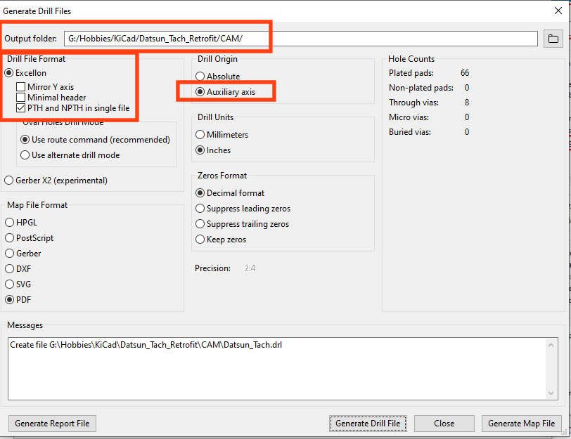
When completed, press Generate Drill Files
Generate Drill Files
Again, leave the Output directory text field empty or pointing to where you want the files to go.
Under Drill File Format, you can combine Plated Through Holes (PTH) and Non-Plated Through Holes (NPTH) into a single file, which I recommend.
Make sure Auxiliary axis is selected
Click the Generate Drill File button to generate the drill file. Note the output in the Messages: box.
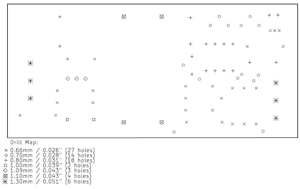
Optionally you can Generate Map File this will show you what drill sizes are used where.
I recommend Generate Report File to give you list of what tool number is what drill size.
Then press Close and Close.
Drill Report
Open the file ”…-drl.rpt” with WordPad. Print. You will need this for tool changes during drilling.
Note: If possible, update your KiCAD footprints to standardize on a limited number of different drill sizes, if possible.
In the example at the right, it was a one-time board, so I didn’t bother to optimize my footprints in KiCAD. Instead I just ‘reduced’ the number of drills during milling. For example, I used a 0.036″ drill for T2, T3, T4 and T5, a 0.050″ drill for T6 and T7. You get the idea.
Drill report for G:HobbiesKiCadDatsun_Tach_RetrofitDatsun_Tach.kicad_pcb
Created on 7/28/2020 4:43:35 PM

Copper Layer Stackup:
==========================================================
L1 : F.Cu front
L2 : B.Cu back
Drill file 'Datsun_Tach.drl' contains
plated through holes:
==========================================================

T1 0.66mm 0.026" (27 holes)
T2 0.70mm 0.028" (14 holes)
T3 0.80mm 0.031" (16 holes)
T4 0.81mm 0.032" (1 hole)
T5 0.83mm 0.033" (1 hole)
T6 1.00mm 0.039" (2 holes)
T7 1.10mm 0.043" (7 holes)
T8 1.30mm 0.051" (6 holes)
Total plated holes count 74

Not plated through holes are merged with plated holes

unplated through holes:
==========================================================
Total unplated holes count 0
Figure 4. Drill Report file.


