EDIT: I have documented the KiCAD to G-code process here: hobbycnc.com/pc_board_isolation_routing/
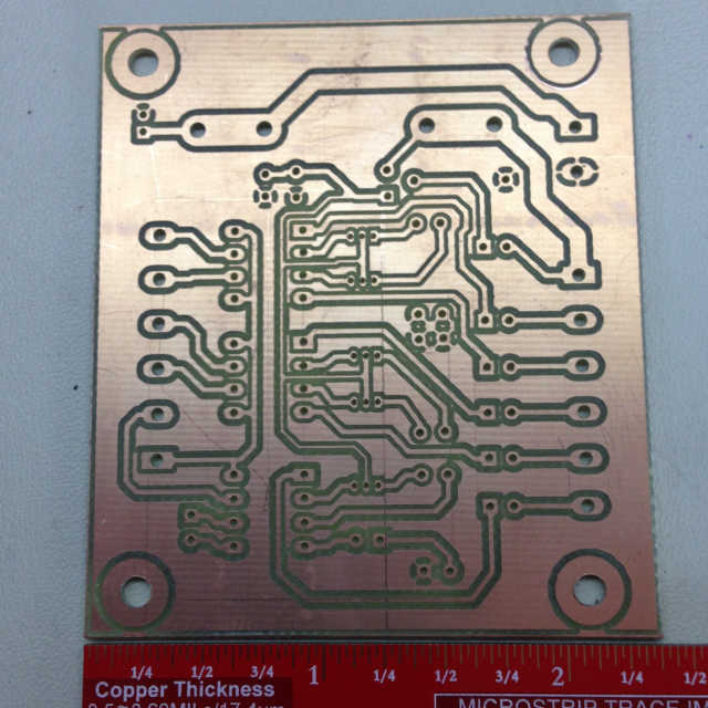
As a follow-up to my last post on Autodesk and Eagle, I did my first PCB isolation routing using the KiCAD and FlatCAM to LinuxCNC toolchain. I did schematic capture and board design on KiCAD and Gerber-to-GCode on FlatCAM. It took a few hours to get somewhat comfortable with the products and process. Obviously, I couldn’t check the PCBs as thoroughly as some of the industrial x ray services out there today because I’m just a hobbyist but I still think I did a decent job. Some of it is still a bit fuzzy to me, but I got it to work anyway.
I ran a ‘pen-test’ of the PCB last night (Video 1). I’ve seen this dozens of times, but it still fascinates me just as much as the x ray checks industrial PCBs go through.
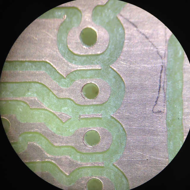
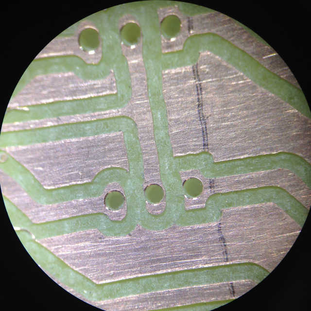
I just finished drilling-and-routing the ‘real thing’ today. I used my new Tapered-stub Trace Isolation Tools from PreciseBits. The results were fantastic. You can see 20x magnification in Figs 2 & 3 – this was right off the machine with no sanding (I did go over it with a stiff, plastic-bristled brush to get off the loose debris).
Overall, I’m pleased with the quality of KiCAD and FlatCAM to produce any type of PCB I’ll ever need. However, for business technology, perhaps using a company like Altium might be in your best interests to make sure that PCB software is created properly.
One final thought – yes, indeed, chemical etching can give much more precise results, and finer geometries, at the added cost of caustic chemicals. Where Isolation Routing wins big-time is the drilling of the holes. Believe-it-or-not, there are just over 100 holes in this damn board!


