PC Board milling (Isolation Routing)
FlatCAM
Introduction
FlatCAM is a great product for converting Gerber files into gcode for milling. However, at first it’s not obvious what all the steps are that need to be done, one-upon-another, to arrive at the final gcode solution.
Here are the main steps:
-
- Import the Gerber and Excellon files.
- “Flip” the board so it is a “bottom view”
- Generate Geometry
- Create tool paths
- convert to gcode
Note: Many (most?) of these settings can be set once in the Options tab. The settings will be saved and become the default on future projects.
Open FlatCAM & Import Gerber Files
Open FlatCAM
File, Open Gerber
-
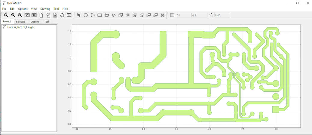
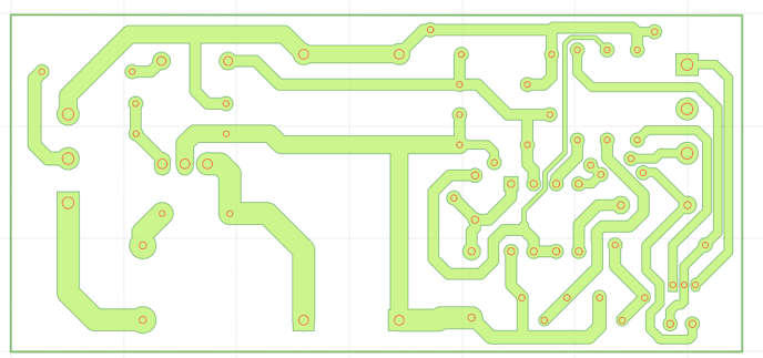
- Open Bottom Copper gerber (Figure 1)
- Open the Edge Cuts gerber (if you have one)
If you have a silk screen file, wait on that for now, we need to do some tricks in KiCad and FlatCAM to get it to work.
File, Open Excellon
-
- Open the drill (.drl) file
Now all files are imported/opened in FlatCAM (Figure 2)
Confirm the origin (0,0) is at the lower left of the board (or wherever you set it in the first KiCad step in the previous section)
Note: We are viewing this board from the top. We want to mill the bottom. In the next step we need to ‘flip over’ the design so we’re looking at the bottom.
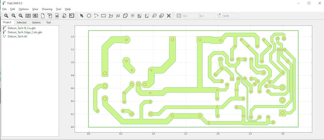
Figure 2 – All 3 Gerber files (bottom copper, edge.cut and drill file) open. TOP VIEW
“Flip” the board over
Each ‘layer’ (bottom copper, holes and edge) need to be flipped individually.
From the Tool menu, select Double-Sided PCB Tool.
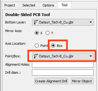
The Tool Tab will open (Figure 3)
- Set the Axis Location to Box
- Select the Bottom Copper Gerber in the Point/Box
- Push Mirror Object
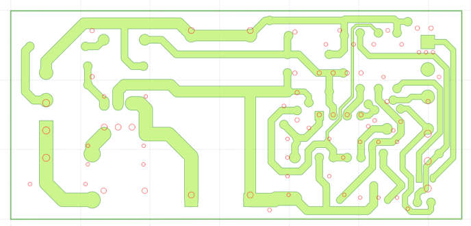
The copper layer has now been ‘flipped’ so we have a bottom view. (Figure 4). Notice that the holes and board edge have not yet been “flipped”
The process needs to be repeated for the holes and the board edge.
Repeat this ‘flipping’ process for all remaining files/layers.
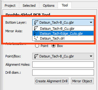
From the Bottom Layer: select the next layer (Figure 5) and press Mirror.
Repeat this one final time for the last layer.
Figure 6 shows the completed result of ‘flipping’ all three files/layers.
Generate Geometry for Copper Layer
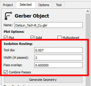
On the Project tab, double-click the Copper layer (…Cu.gbr).
Tool dia: The diameter of your tool at the specified cutting depth. Use the Tool Width Calculator to figure out the width (for ‘V’ shaped cutting tools).
Width (#passes): Each successive pass moves ‘out’ a little farther. I have good luck with 2.
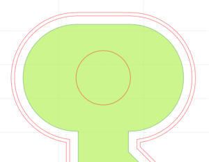
Pass overlap: I have good results at 60% (0.60). See “Some examples of Width and Pass Overlap” section, below for details on pass overlap.
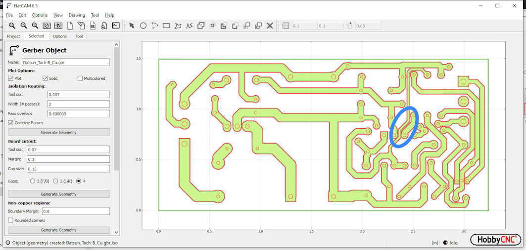
Push Generate Geometry when done.
The red lines around every traceindicate where the tool will cut. Inspect it carefully, especially areas where traces are close to each other – see blue circle. Also see “Some examples of Width and Pass Overlap“, below.
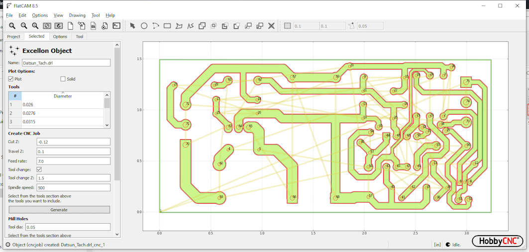
Generate Geometry for Holes
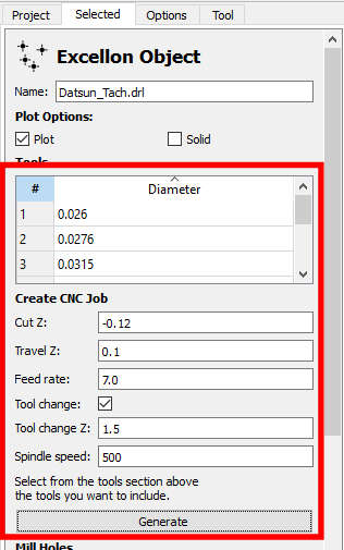
On the Project tab, double-click the drill (.drl) layer.
Tools – just be sure all the tools are selected (Hashtag is highlighted with blue background = all drill selected). This is the default. Any tool unselected will not be drilled.
Cut Z – how deep below the surface of the copper you will drill. This needs to be a bit deeper than the thickness of your PC board stock.
Travel Z – how far up the tool will retract when moving between cuts.
Feed Rate – Plunge speed of the tool as it goes through the board.
Tool Change – check this and set the Tool change Z (I find 1.5 inches works well) to allow space to change the drills.
Spindle Speed – must be positive number if you have spindle control.
Push Generate Geometry when done.
The holes will be added.
Generate Geometry for Board Edge
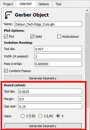
On the Project tab, double-click the edge cuts (..Edge_Cuts.gbr) layer.
Tool dia – the diameter of the cutout bit. This is a side-cutting (router) bit, not just a drill and not the ‘V’ cutter.
Margin – extra space around the margin of the board. Zero will cut the board to the exact size.
Gap Size – the size of the holding tabs around the board perimeter. Zero for no holding tabs (not recommended)
Gaps – Number and location of where you want the holding tabs.
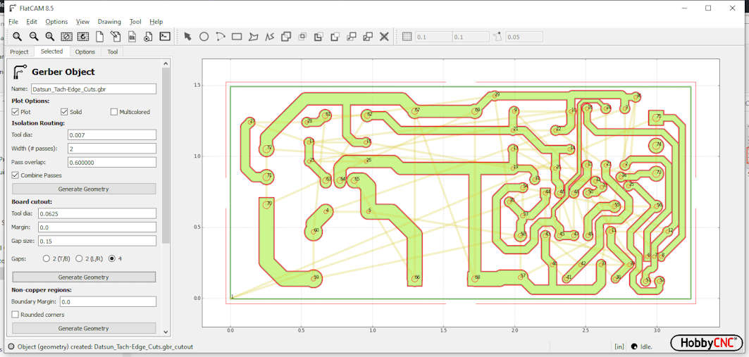
Push Generate Geometry when done.
The red lines around the perimeter indicate where the tool will cut. This line represents the center of the cutting tool.
Notice four ‘gaps’ in the red line around the perimeter of the board – these are the holding tabs (Gaps).
Create Tool Paths
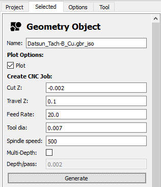
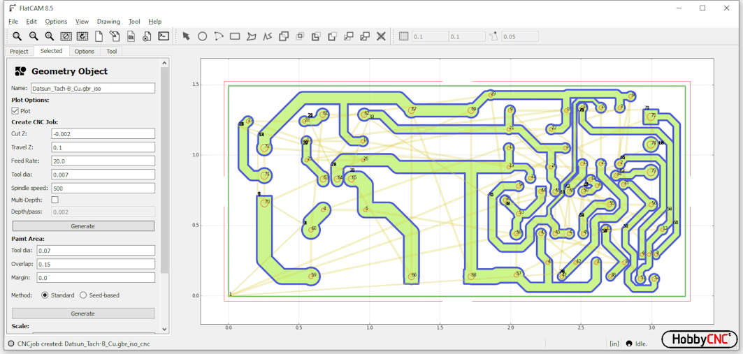
From the Project tab, double-click the ..B-Cu.gbr_iso.
Cut Z – how deep below the surface of the copper you will mill. This needs to be a just a tiny bit deeper than the thickness of the copper.
Travel Z – how far up the tool will retract when moving between cuts.
Feed Rate – Cutting speed of the tool as it cuts the isolation tracks on the board.
Tool dia – the cutting width of the tool (see Tool Width Calculator to determine the width of ‘V’ shaped cutting tools.
Spindle Speed – must be positive number if you have spindle control.
The red lines (which indicate the center of the tool) are replaced with blue lines that indicate the actual copper material removed.
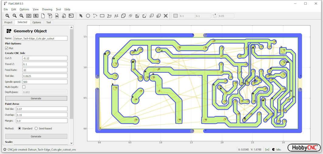
Tool Path Edge Cuts
Open the Project tab and double-click on the …Edge_Cuts.gbr.
Tool dia – the diameter of the cutout bit. This is a side-cutting (router) bit, not just a drill and not the ‘V’ cutter.
Margin – extra space around the margin of the board. Zero will cut the board to the exact size.
Push Generate Geometry.
The red line around the perimeter will be replaced with a blue line representing the location and width of the cutting tool.
Final Steps: Convert to gcode
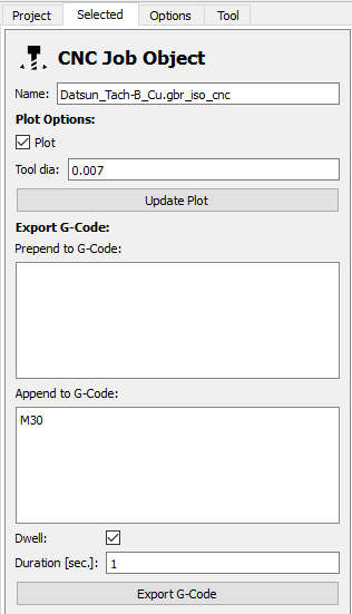
On the Project tab, select the _Cu.gbr_iso_cnc file.
The only step here is to press Export G-Code. You will be prompted where to save the file.
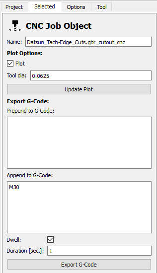
Note: I use LinuxCNC, which requires the gcode to end with an M30 (end of program). Could probably use M2 also.
You can add ‘stuff’ to the beginning (Prepend) or the end (Append) of the gcode that is generated.
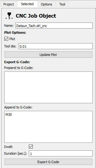
Convert to gcode – Drill
Return to the Project tab and repeat the above for the .drl_cnc file
Convert to gcode board edge
Return to the Project tab and repeat the above for the Edge_Cuts.gbr_cutout_cnc file
Done
These steps go quite quickly once you get the hang of it.
You will now have two (or three if you have edge cuts) gcode files. One for the bottom copper, one for the drilling and optionally one for the edge cuts.
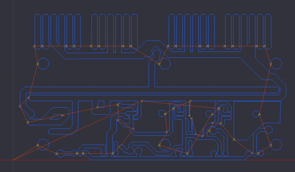
I STRONGLY RECOMMEND double-checking the gcode in a gcode viewer before moving on.
Some examples of Width and Pass Overlap
|
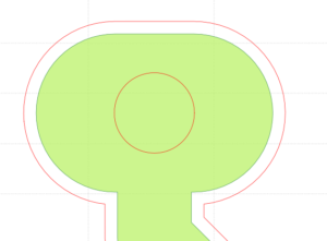
One pass (overlap is not relevant) |
 |
|
|
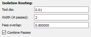
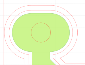
Pass overlap = 80% overlap. (100% overlap would look exactly like the image above) |
 |
|
|
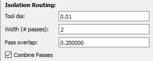
Pass overlap = 20% |
 |
|
|
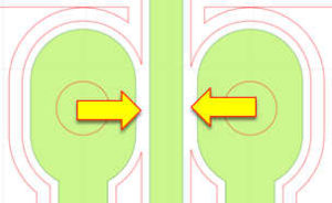
Look for incomplete passes You will need to: |
 |
Verify GcodeOpen the gcode files in a viewer (I use CamBam) to verify.
|
|
|
Verify drill file in gcode viewer
|
